Exploring the Micro World – Key Publications

This publication presents a high-impact collaboration between NVIDIA and NenoVision, showcasing how AFM-in-SEM technology fundamentally extends the capabilities of advanced semiconductor failure analysis. In the paper, Chuan Zhang, Lead Failure Analysis Engineer at NVIDIA, provides a clear and practice-driven explanation of why conventional SEM-based techniques often fall short at advanced …

Electron-Beam Excited Conductive AFM: Back-Contact-Free Electrical Characterization for Advanced Failure Analysis and Wafer-Scale 2D Materials
This publication presents a novel electrical atomic force microscopy technique—Electron-Beam Excited Conductive AFM (EBC-AFM)—that introduces a fundamentally new approach to electrical characterization and failure analysis of advanced materials. In this method, a low-energy electron beam is used to inject charge directly into the material, while local conductivity is mapped using …
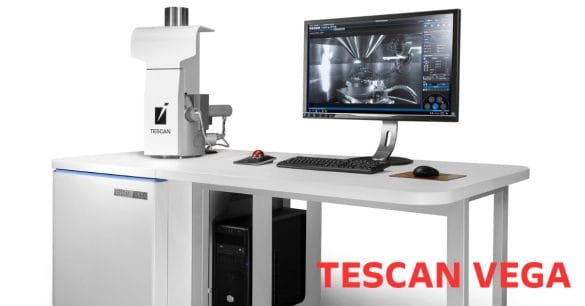
The TESCAN VEGA scanning electron microscope combines versatility with reliability, making it an essential tool in a wide range of scientific and industrial applications. The following publications highlight research where the TESCAN VEGA played a central role in imaging, material characterization, and surface analysis.
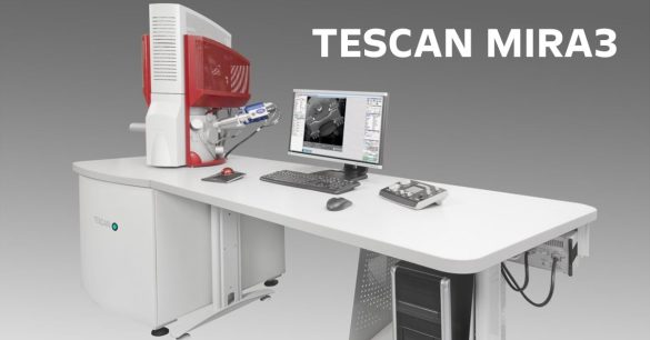
The TESCAN MIRA3 scanning electron microscope has been instrumental in numerous scientific studies, providing high-resolution imaging and detailed surface analysis. Below is a selection of scientific publications where this advanced instrument played a key role in the research and results.