
In-situ Nanoprobing Solutions for SEM, FIB and DualBeam Microscopes
High-precision robotic nanoprobing for semiconductor failure analysis, electrical characterization and nanomanipulation.
The IMINA NANO Product Line brings advanced nanoprobing capabilities directly into scanning electron microscopes (SEM), focused ion beam (FIB) systems and DualBeam instruments. Designed for both research laboratories and semiconductor manufacturing, the platform enables precise electrical measurements, defect localization and nanomanipulation with exceptional speed, stability and repeatability.
Whether you are characterizing advanced semiconductor devices, performing Electrical Failure Analysis (EFA), or manipulating individual nanostructures, the NANO platform provides a flexible solution that integrates seamlessly into existing microscopy workflows.
KEY BENEFITS
Nanometer Precision
Achieve highly accurate positioning and reliable electrical contact with nanometer-scale resolution.
Flexible Multi-Robot System
Configure up to eight independently controlled robots to perform complex probing and manipulation tasks.
Fast & Stable Operation
Piezoelectric actuation provides rapid positioning, exceptional stability and minimal drift during long experiments.
SEM, FIB & DualBeam Ready
Designed for seamless integration with most electron microscopes without permanent modifications.
Automated Workflows
The Precisio™ Software Suite simplifies positioning, measurements and experiment automation.
Modular & Expandable
Easily customize the platform with probes, grippers, stages and accessories for your specific application.
Typical Applications
The IMINA NANO platform is widely used for:
- Semiconductor Electrical Failure Analysis (EFA)
- In-situ nanoprobing
- Electrical characterization of integrated circuits
- Wafer and chip debugging
- EBIC / EBAC / RCI measurements
- MEMS and NEMS characterization
- Nanowire measurements
- Materials science research
- Device reliability studies
- Nanomanipulation inside SEM
- Sample preparation
- Temperature-dependent electrical characterization
Built Around the Unique miBot™ Robot
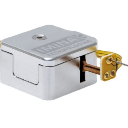
At the heart of every NANO system is the patented miBot™ nanoprobing robot.
Unlike conventional micromanipulators, miBot™ is a compact mobile robot driven by piezoelectric actuators. This unique design allows both rapid coarse positioning over centimeter distances and ultra-fine nanometer-scale motion, while maintaining exceptional stability throughout the experiment.
Its compact size also allows operation in demanding SEM environments, including:
- Magnetic immersion mode
- Short working distances
- High tilt angles
- Simultaneous FIB processing and electrical probing
Optional Modules
The NANO platform can be configured with a wide range of accessories, including:
- Sample XYZ positioning stage
- Large sample adapter
- High-performance Electrical Failure Analysis modules
- Thermal stage (-30°C to +150°C)
- NANO+ extended Z fine-motion robot
- Optical fiber positioning
- Custom OEM integrations
The modular architecture allows the system to grow together with your research or production requirements.
WHY CHOOSE IMINA
Swiss engineering, patented robotic technology and intuitive software make IMINA one of the world’s leading providers of nanoprobing solutions for semiconductor analysis.
Researchers, universities, failure analysis laboratories and semiconductor manufacturers worldwide rely on IMINA systems for accurate measurements, reduced setup times and maximum experimental flexibility.
Request More Information
Looking for the ideal nanoprobing solution for your SEM or FIB system?
Our specialists will help you configure the optimal IMINA NANO system for your microscope, applications and measurement requirements.
Contact us
Tel: +36-30-225-7704
Skype: patricia.varju; ImageScience
Address: Greszl Ferenc street 27, Nagykovacsi, H-2094, Hungary