
PRECISION SOLUTIONS FOR SEMICONDUCTOR FAILURE ANALYSIS & PROCESS CONTROLL
Advanced analytical solutions for the final stage of the semiconductor value chain — from failure analysis to packaging inspection and reliability qualification.
Image-Science connects semiconductor manufacturers, foundries, and research labs in Hungary with specialized analytical instrumentation for failure analysis, process control, and reliability testing. While front-end wafer fabrication relies on its own dedicated toolset, our expertise centers on the critical final phase of the semiconductor workflow.
Semiconductor Failure Analysis & Process Control
— Our Focus Areas
Supporting the final phase of the semiconductor workflow with advanced failure analysis, characterization, and reliability technologies.
1
FIB-SEM Failure Analysis & Sample Preparation
Locate and Isolate Faults Without Compromising the Device
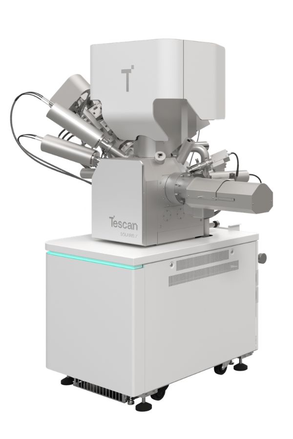
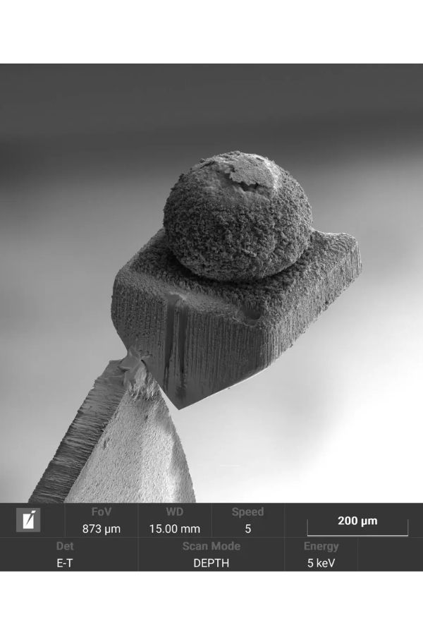
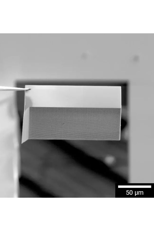
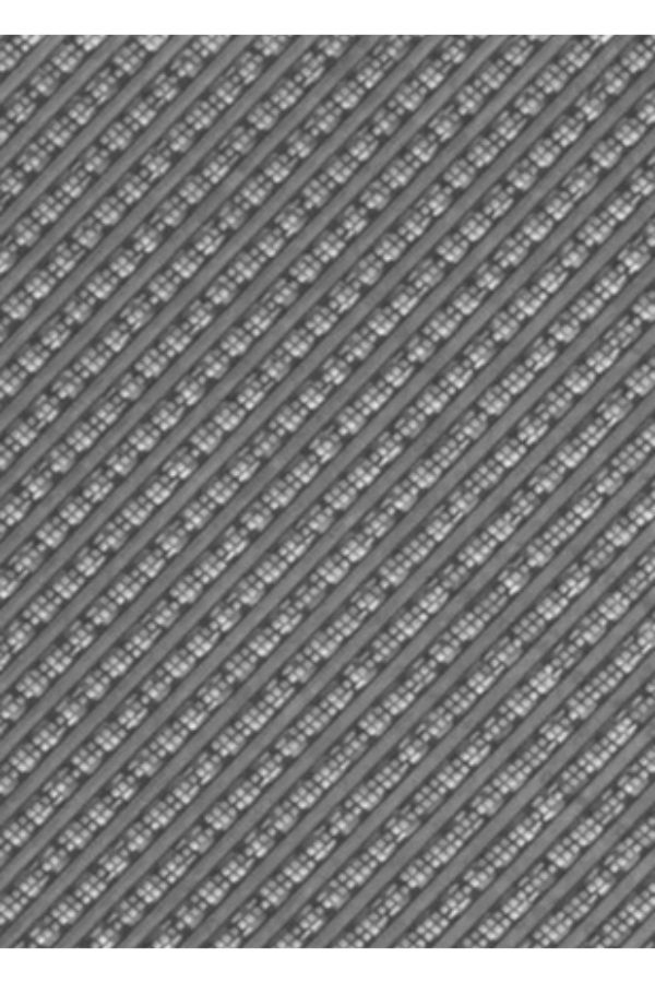
Modern packaged and wafer-level devices demand failure analysis workflows that preserve fragile structures while delivering reproducible results. Combining plasma and gallium FIB-SEM systems with CAD-assisted navigation, these solutions support delayering, artifact-free cross-sectioning, and TEM lamella preparation for even the most complex packages — from BGAs and TSVs to MEMS and bond wires.
- FIB-SEM Delayering & Cross-Sectioning (Plasma & Ga+ FIB)
- TEM Lamella Preparation
- CAD-Assisted Navigation & Endpoint Detection
- 4D-STEM Phase & Crystallographic Mapping
- Micro-CT Non-Destructive 3D Imaging
2
Correlative AFM Failure Analysis
See Structure and Electrical Behavior in a Single Vacuum Cycle
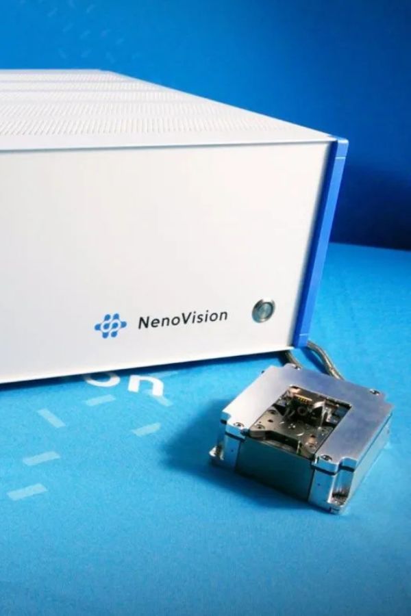
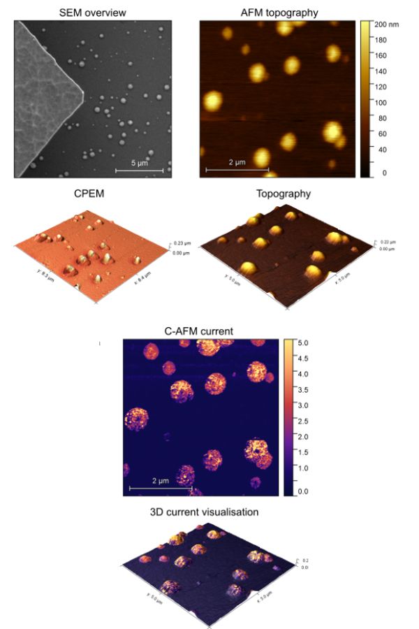
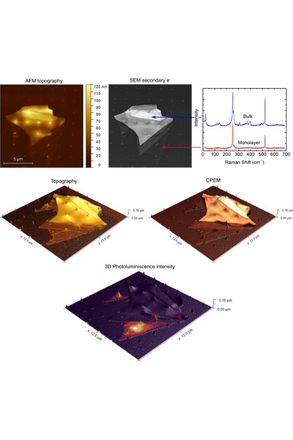
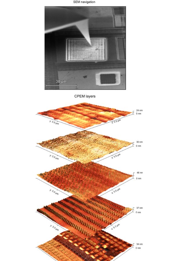
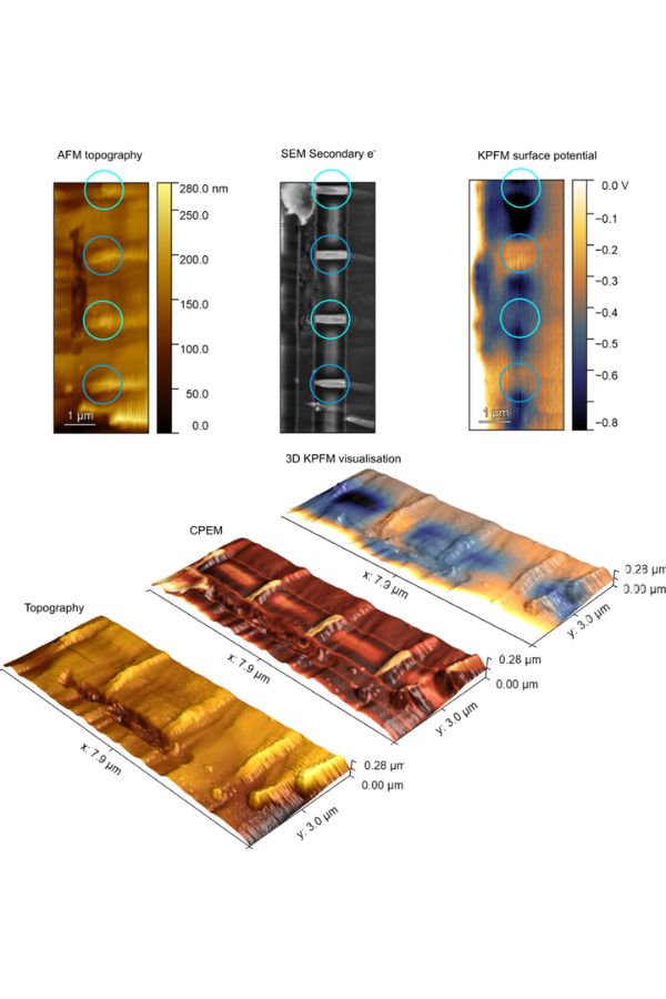
Integrating atomic force microscopy directly into the SEM/FIB chamber lets you correlate topography with electrical measurements without breaking vacuum — critical for NAND flash, SRAM, logic, FinFET and CMOS devices, where oxidation or repeated sample transfer can obscure the fault. Conductive AFM, electrical spectroscopy, and scanning spreading resistance microscopy (SSRM) reveal dopant profiles and defects layer by layer.
- AFM-in-SEM Correlative Microscopy
- Conductive AFM & Electrical Spectroscopy
- Scanning Spreading Resistance Microscopy (SSRM)
- Layer-by-Layer NAND & Transistor Analysis
3
Nanoprobing & Electrical Characterization
Nanometer-Precision Probing Inside the Microscope
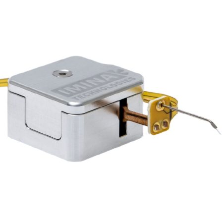
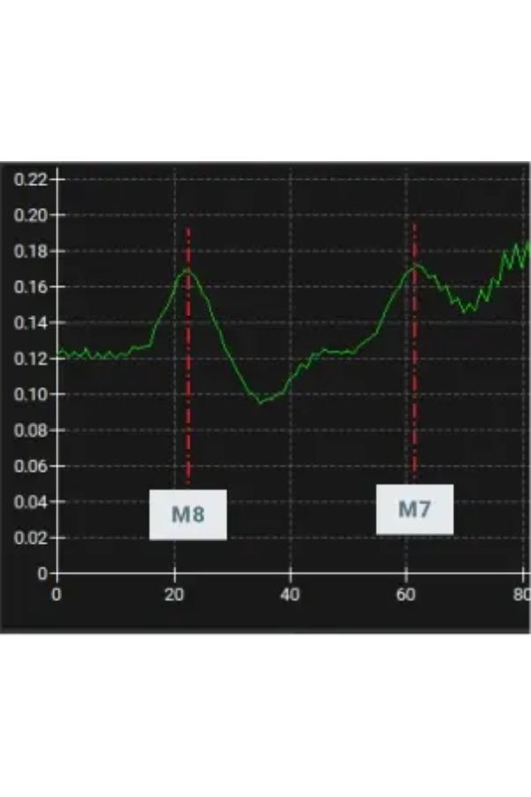
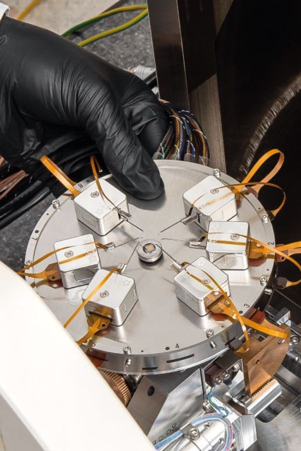
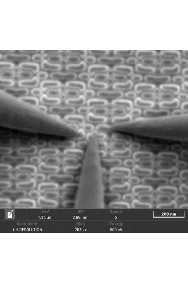
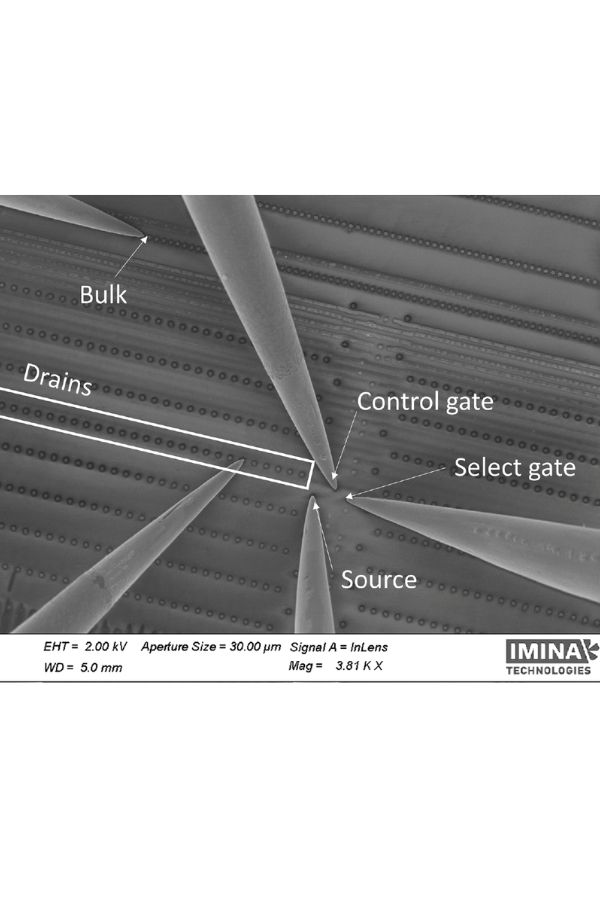
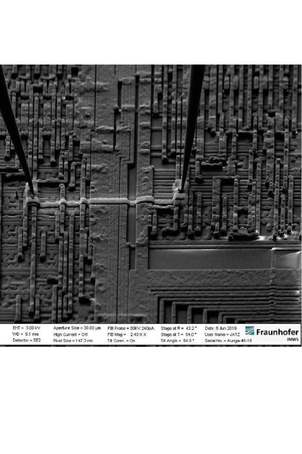
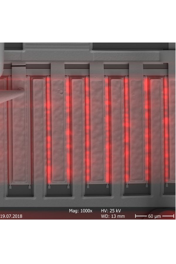
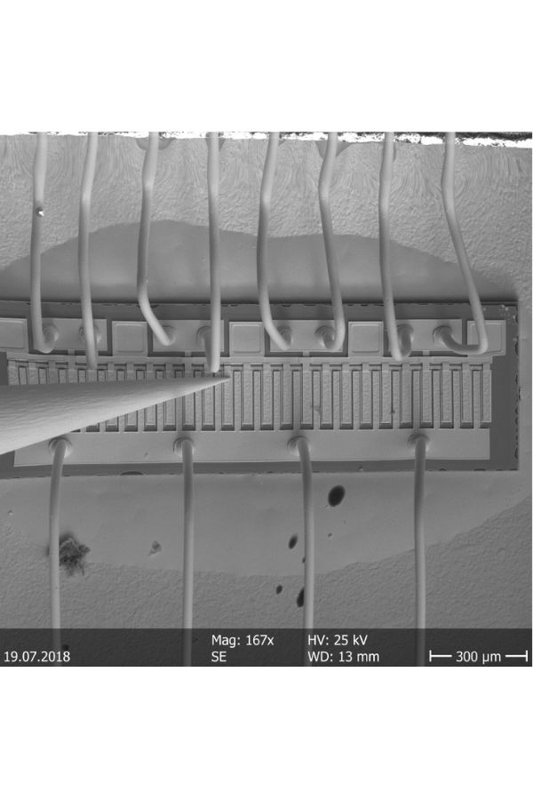
Robotic nanoprobing platforms provide direct electrical access to transistors and interconnects at advanced technology nodes (down to 5 nm), enabling EBIC, EBAC, EBIRCh, and resistance contrast imaging (RCI) directly inside the electron or optical microscope. From PMOS/NMOS characterization to memory debug, nanowire probing, and MEMS/NEMS testing, these systems bring precise, repeatable electrical characterization to devices too small for manual probing.
- Robotic Nanoprobing (NANO & MICRO Platforms)
- EBIC / EBAC / EBIRCh / Resistance Contrast Imaging (RCI)
- PMOS/NMOS & Memory Device Characterization
- MEMS/NEMS & Photonics (microLED) Testing
Solutions available through our partner Imina Technologies.
4
Raman Spectroscopy for Material & Stress Analysis
Non-Destructive Insight into Composition, Structure and Stress
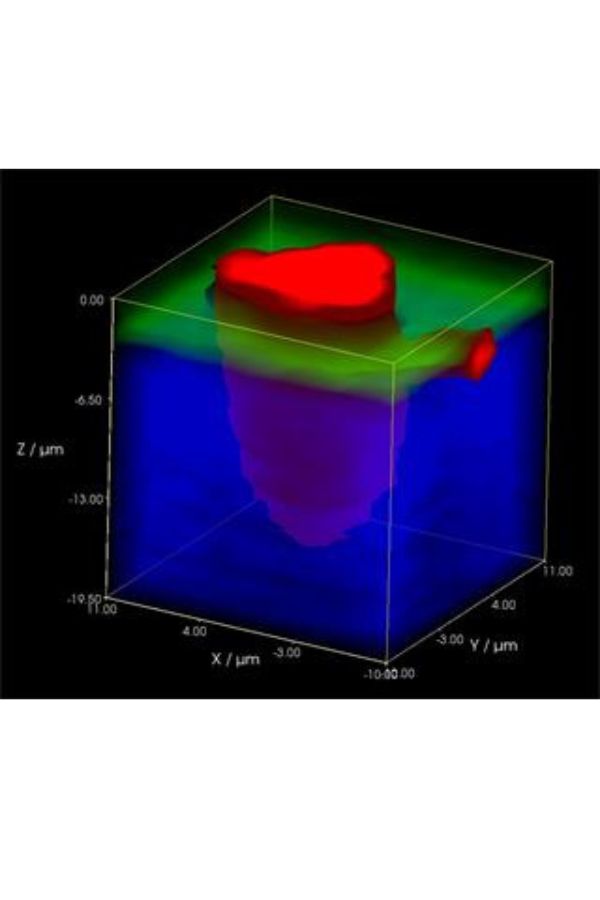
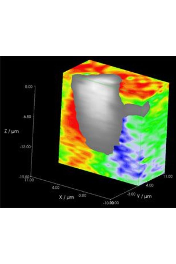
Raman spectroscopy analyzes transistors, compound semiconductors, solar cells and LEDs without sample preparation, vacuum, or charging effects. It identifies chemical composition and alloy fractions, distinguishes polytypes and crystal quality, maps compressive and tensile stress around defects, and profiles dopant concentration, thin-film thickness, and uniformity.
- Material & Alloy Composition Identification
- Polytype & Crystal Quality Analysis
- Stress / Strain Mapping
- Dopant Concentration & Thin-Film Thickness
- In-Line Wafer Scanning for Yield Improvement

5
Reliability & Environmental Stress Testing
Qualify Devices Before They Reach the Field
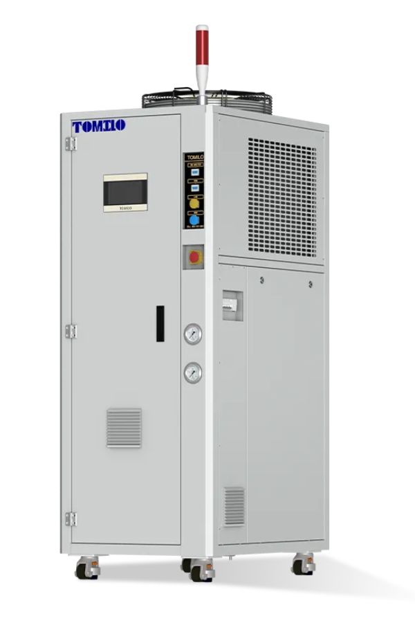
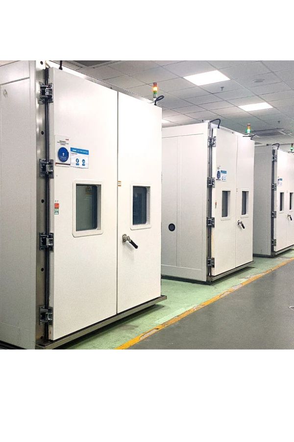
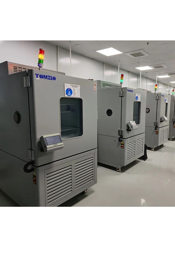
Environmental and thermal stress testing exposes design and process defects before products ship. Temperature & humidity chambers, rapid temperature change chambers, and two- and three-zone thermal shock chambers simulate the conditions semiconductor components and consumer electronics devices will face in the field.
- Temperature & Humidity Testing
- Rapid Temperature Change / Environmental Stress Screening
- Two- and Three-Zone Thermal Shock Testing
6
X-Ray & CT Package Inspection
Non-Destructive 3D Insight into Packaged Devices
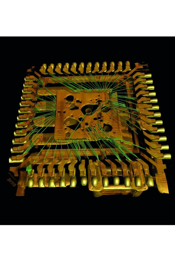
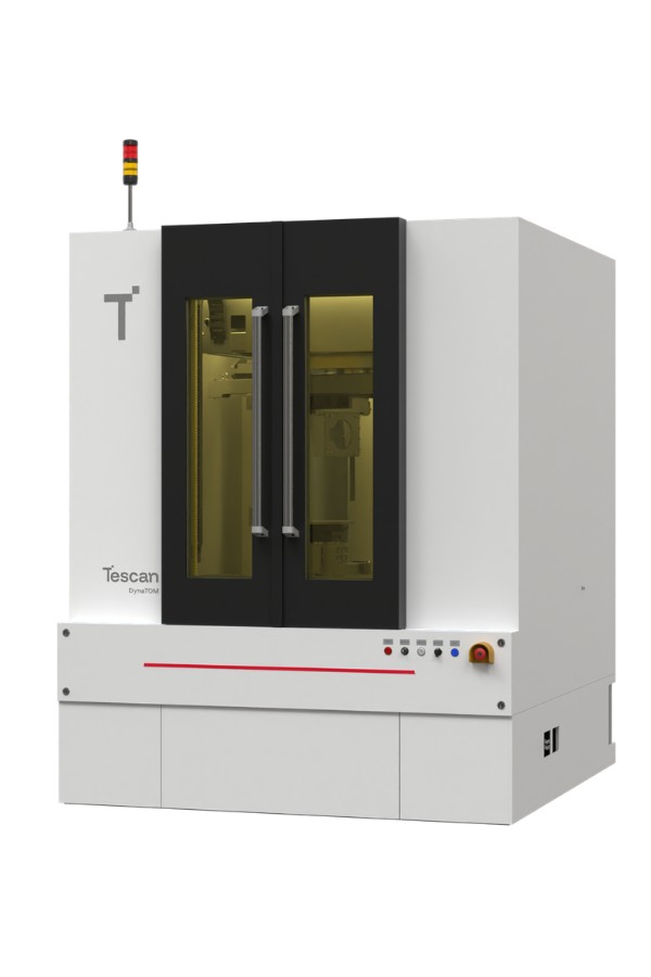
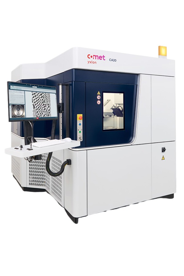
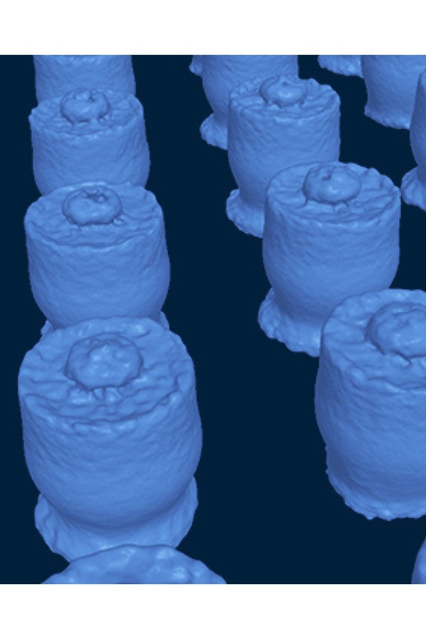
X-ray and computed tomography reveal internal solder joints, wire bonds, voids, and package integrity without opening the device — ideal for BGA, TSV, and multi-die package inspection.
- X-Ray Inspection
- Computed Tomography (CT) 3D Imaging
- Void, Voiding & Bond Wire Analysis
Why Image-Science
Your partner for semiconductor failure analysis & reliability
Curated Technology Portfolio
We evaluate and select specialized technology partners, so you don’t have to vet every vendor yourself.
Local Expertise, Global Technology
We bring leading international failure-analysis technology together with local, Hungarian-based application support.
Correlative & Non-Destructive Analysis
Combine structural, electrical, and chemical insight from a single, minimally invasive workflow.
Application Expertise
Our specialists help you select the right technique for your specific device and failure mode.
Ready to Solve Your Next SEMICONDUCTOR failure Analysis Challenge?
Whether you are debugging a field return, qualifying a new package, or building out an in-house failure analysis lab, our experts can help you find the right analytical solution.
Contact us
Tel: +36-30-225-7704
Skype: patricia.varju; ImageScience
Address: Greszl Ferenc street 27, Nagykovacsi, H-2094, Hungary